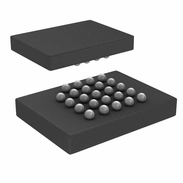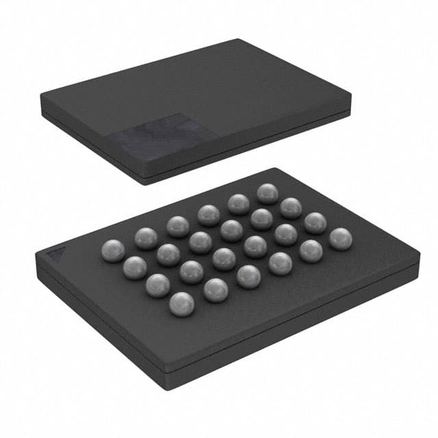
S25FL512SDPBHB210 Cypress Semiconductor Corp NOR
Интегральные схемы (ИС) -
Номер производителя:
S25FL512SDPBHB210
Производитель:
Категория продукции:
Описание:
NOR
Состояние RoHs:
Таблицы данных:
Access Time :
-
Clock Frequency :
-
Memory Format :
-
Memory Interface :
-
Memory Size :
-
Memory Type :
-
Mounting Type :
-
Operating Temperature :
-
Package / Case :
-
Packaging :
-
Part Status :
Active
Series :
Supplier Device Package :
-
Technology :
-
Voltage - Supply :
-
Write Cycle Time - Word, Page :
-
в наличии
14,365
Unit Price:
Свяжитесь с нами
Предложение
S25FL512SDPBHB210 Конкурентные цены
ChipIc имеет уникальный источник поставок. Мы можем предложить S25FL512SDPBHB210 более
конкурентоспособную цену для наших клиентов. Вы можете насладиться нашим лучшим
сервисом, купив ChipIc S25FL512SDPBHB210. Пожалуйста, не стесняйтесь обращаться по поводу
лучшей цены на S25FL512SDPBHB210. Нажмите, чтобы получить предложение
S25FL512SDPBHB210 Особенности
S25FL512SDPBHB210 is produced by Cypress Semiconductor Corp, belongs to объем памяти, and its best working temperature is -, the size is -, and - is its most common packaging method, which belongs to the series, using -, - is the most suitable voltage.
S25FL512SDPBHB210 Подробная информация о продукции
:
S25FL512SDPBHB210 — это объем памяти, буферные усилители, разработанные и
произведенные
Cypress Semiconductor Corp.
S25FL512SDPBHB210 производства Cypress Semiconductor Corp можно приобрести на сайте CHIPMLCC.
Здесь вы можете найти различные виды электронных деталей от ведущих производителей мира.
S25FL512SDPBHB210 компании CHIPMLCC прошел строгий контроль качества и соответствует всем требованиям.
Статус запасов, отмеченный на CHIPMLCC, предназначен только для справки.
Если вы не нашли запчасть, которую ищете, вы можете связаться с нами для получения дополнительной информации, такой как количество запасов в таблице данных S25FL512SDPBHB210 (PDF), цена S25FL512SDPBHB210, Распиновка S25FL512SDPBHB210, руководство S25FL512SDPBHB210 и решение на замену S25FL512SDPBHB210.
S25FL512SDPBHB210 FAQ
:
1. What is the maximum clock frequency of the S25FL512SDPBHB210?
The maximum clock frequency of the S25FL512SDPBHB210 is 133 MHz.
2. What is the operating voltage range of the S25FL512SDPBHB210?
The operating voltage range of the S25FL512SDPBHB210 is 2.7V to 3.6V.
3. What is the typical power consumption of the S25FL512SDPBHB210 during read operations?
The typical power consumption of the S25FL512SDPBHB210 during read operations is 4 mA.
4. Can the S25FL512SDPBHB210 perform sector erase operations?
Yes, the S25FL512SDPBHB210 can perform sector erase operations.
5. What is the maximum data transfer rate of the S25FL512SDPBHB210 in Quad SPI mode?
The maximum data transfer rate of the S25FL512SDPBHB210 in Quad SPI mode is 532 MB/s.
6. Does the S25FL512SDPBHB210 support software and hardware write protection?
Yes, the S25FL512SDPBHB210 supports both software and hardware write protection features.
7. What is the temperature range for the S25FL512SDPBHB210's operation?
The S25FL512SDPBHB210 is designed to operate within a temperature range of -40°C to 85°C.
8. How many erase cycles can the S25FL512SDPBHB210 endure?
The S25FL512SDPBHB210 can endure up to 100,000 erase cycles per sector.
9. What is the size of the S25FL512SDPBHB210's memory array?
The S25FL512SDPBHB210 has a memory array size of 64 Mb (8 MB).
10. Is the S25FL512SDPBHB210 RoHS compliant?
Yes, the S25FL512SDPBHB210 is RoHS compliant.
S25FL512SDPBHB210 Связанные ключевые слова
:
S25FL512SDPBHB210 Цена
S25FL512SDPBHB210 Картина
S25FL512SDPBHB210 Напряжение на выводе
Акции: Быстрая проверка котировок
Минимальный заказ: 1
Contains
"S25F"
series
products