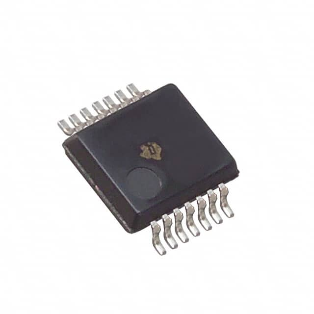
SN74LVC574ADWR Texas Instruments IC FF D-TYPE SNGL 8BIT 20SOIC
Интегральные схемы (ИС) 20-SOIC (0.295", 7.50mm Width)
Номер производителя:
SN74LVC574ADWR
Производитель:
Категория продукции:
Описание:
IC FF D-TYPE SNGL 8BIT 20SOIC
Состояние RoHs:
Таблицы данных:
Clock Frequency :
150MHz
Current - Output High, Low :
24mA, 24mA
Current - Quiescent (Iq) :
1.5µA
Function :
Standard
Input Capacitance :
4pF
Max Propagation Delay @ V, Max CL :
6.8ns @ 3.3V, 50pF
Mounting Type :
Surface Mount
Number of Bits per Element :
8
Number of Elements :
1
Operating Temperature :
-40°C ~ 125°C (TA)
Output Type :
Tri-State, Non-Inverted
Package / Case :
20-SOIC (0.295", 7.50mm Width)
Packaging :
Tape & Reel (TR)
Part Status :
Active
Series :
74LVC
Trigger Type :
Positive Edge
Type :
D-Type
Voltage - Supply :
1.65 V ~ 3.6 V
в наличии
22,995
Unit Price:
Свяжитесь с нами
Предложение
SN74LVC574ADWR Конкурентные цены
ChipIc имеет уникальный источник поставок. Мы можем предложить SN74LVC574ADWR более
конкурентоспособную цену для наших клиентов. Вы можете насладиться нашим лучшим
сервисом, купив ChipIc SN74LVC574ADWR. Пожалуйста, не стесняйтесь обращаться по поводу
лучшей цены на SN74LVC574ADWR. Нажмите, чтобы получить предложение
SN74LVC574ADWR Особенности
SN74LVC574ADWR is produced by Texas Instruments, belongs to Логика - Flip Flops, and its best working temperature is -40°C ~ 125°C (TA), the size is 20-SOIC (0.295", 7.50mm Width), and Tape & Reel (TR) is its most common packaging method, which belongs to the 74LVC series, 1.65 V ~ 3.6 V is the most suitable voltage.
SN74LVC574ADWR Подробная информация о продукции
:
SN74LVC574ADWR — это Логика - Flip Flops, буферные усилители, разработанные и
произведенные
Texas Instruments.
SN74LVC574ADWR производства Texas Instruments можно приобрести на сайте CHIPMLCC.
Здесь вы можете найти различные виды электронных деталей от ведущих производителей мира.
SN74LVC574ADWR компании CHIPMLCC прошел строгий контроль качества и соответствует всем требованиям.
Статус запасов, отмеченный на CHIPMLCC, предназначен только для справки.
Если вы не нашли запчасть, которую ищете, вы можете связаться с нами для получения дополнительной информации, такой как количество запасов в таблице данных SN74LVC574ADWR (PDF), цена SN74LVC574ADWR, Распиновка SN74LVC574ADWR, руководство SN74LVC574ADWR и решение на замену SN74LVC574ADWR.
SN74LVC574ADWR FAQ
:
1. What is the operating voltage range for the SN74LVC574ADWR?
The operating voltage range for the SN74LVC574ADWR is 2 V to 3.6 V.
2. What is the maximum input clamp current for this device?
The maximum input clamp current for the SN74LVC574ADWR is ±20 mA.
3. Can this device be used in a daisy-chain configuration?
Yes, the SN74LVC574ADWR can be used in a daisy-chain configuration for serial data transfer.
4. What is the typical output rise/fall time for this latch?
The typical output rise/fall time for the SN74LVC574ADWR is 0.8 ns.
5. Is the SN74LVC574ADWR compatible with 5V TTL/CMOS logic levels?
Yes, this device is compatible with 5V TTL/CMOS logic levels when used with appropriate level-shifting techniques.
6. What is the maximum propagation delay for the SN74LVC574ADWR?
The maximum propagation delay for this latch is 5.3 ns.
7. Can the SN74LVC574ADWR withstand electrostatic discharge (ESD)?
Yes, this device has ESD protection and can withstand up to 2000 V human-body model (HBM) ESD.
8. What is the maximum quiescent current consumption of the SN74LVC574ADWR?
The maximum quiescent current consumption of this latch is 10 µA at 25°C.
9. Does the SN74LVC574ADWR have an integrated output diode for inductive load protection?
No, this device does not have an integrated output diode for inductive load protection.
10. What is the package type and dimensions for the SN74LVC574ADWR?
The SN74LVC574ADWR is available in a SOIC-20 package with dimensions of 12.8 mm x 7.5 mm.
SN74LVC574ADWR Связанные ключевые слова
:
SN74LVC574ADWR Цена
SN74LVC574ADWR Картина
SN74LVC574ADWR Напряжение на выводе
Акции: Быстрая проверка котировок
Минимальный заказ: 1
Contains
"SN74"
series
products